
Part №
(Код ЗЧД=Номер ЗЧД)
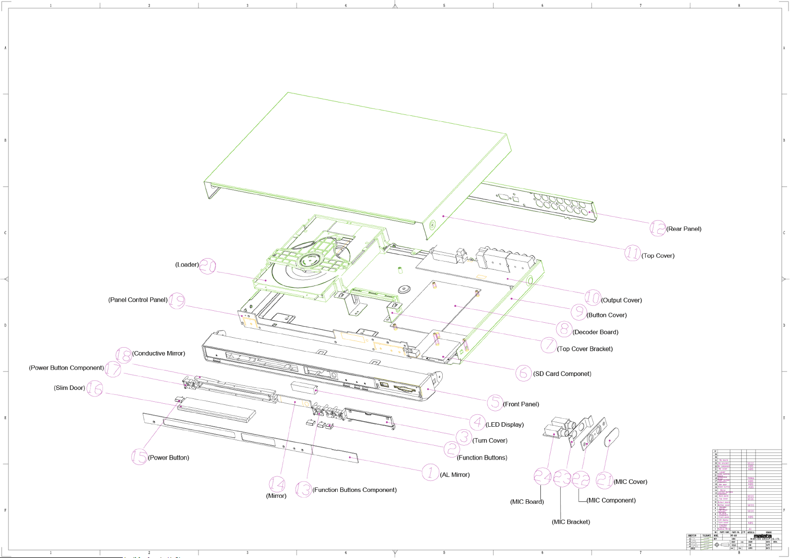
1 AL Mirror
1 DV-550-1
2 Function Buttons
1 DV-550-2
3 Turn Cover
1 DV-550-3
4 LED Display
1 DV-550-4
5 Front Panel
1 DV-550-5
6 SD Card Componet
1 DV-550-6
7 Top Cover Bracket
1 DV-550-7
8 Decoder Board (MAINBOARD)
1 DV-550-8
9 Button Cover
1 DV-550-9
10 Output Cover (OUTPUT BOARD)
1 DV-550-10
11 Top Cover
1 DV-550-11
12 Rear Panel
1 DV-550-12
13 Function Buttons Component
1 DV-550-13
14 Mirror
1 DV-550-14
15 Power Button
1 DV-550-15
16 Slim Door
1 DV-550-16
17 Power Button Component
1 DV-550-17
18 Conductive Mirror
1 DV-550-18
19 Panel Control Panel
1 DV-550-19
20 Loader
1 KHM-313AAA
21 MIC Cover
1 DV-550-21
22 MIC Component
1 DV-550-22
23 MIC Bracket
1 DV-550-23
24 MIC Board (KARAOKE BOARD)
1 DV-550-24
Remote Control
1 DV-550-25
POWER BOARD
1 DV-550-26
FRONT BOARD
1 DV-550-27
Spare Parts List (DV-550)
DescriptionItem QTY
Part №
(Код ЗЧД=Номер ЗЧД)
1 AL Mirror
1 DV-560-1
2 Function Buttons
1 DV-560-2
3 Turn Cover
1 DV-560-3
4 LED Display
1 DV-560-4
5 Front Panel
1 DV-560-5
6 SD Card Componet (CARDREAD BOARD)
1 DV-560-6
7 Top Cover Bracket
1 DV-560-7
8 Decoder Board (MAINBOARD)
1 DV-560-8
9 Button Cover
1 DV-560-9
10 Output Cover (OUTPUT BOARD)
1 DV-560-10
11 Top Cover
1 DV-560-11
12 Rear Panel
1 DV-560-12
13 Function Buttons Component
1 DV-560-13
14 Mirror
1 DV-560-14
15 Power Button
1 DV-560-15
16 Slim Door
1 DV-560-16
17 Power Button Component
1 DV-560-17
18 Conductive Mirror
1 DV-560-18
19 Panel Control Panel
1 DV-560-19
20 Loader
1 KHM-313AAA
21 MIC Cover
1 DV-560-21
22 MIC Component
1 DV-560-22
23 MIC Bracket
1 DV-560-23
24 MIC Board (KARAOKE BOARD)
1 DV-560-24
Remote Control
1 DV-560-25
POWER BOARD
1 DV-560-26
FRONT BOARD
1 DV-560-27
Spare Parts List (DV-560)
DescriptionItem QTY

SERVICE MANUAL
MODEL:DV550/DV560
CONTENT
PART 1: Brief Introduction
◆ Speciation
◆ Schematic Diagram
PART 2: Key Ics And Assemblies
PART 3: Detailed Circuit
◆
Panel Board(attached drawing)
◆
Power Board(attached drawing)
◆
Main Board(attached drawing)
P
A
R
T
4
:
P
a
r
t
s
L
ist
PART 5: Debug Procedure
Part 1 Brief Introduction
hank you for buying
ELENBERG DVD Product. As a high—resolution DVD
player,
The DVD offers the high quality of DVD playback from a
sleek, portable chassis. It plays almost all kinds of discs such as DVD-video, video
CD, CD-R, CD-RW, MP3,WMA,PICTURE—CD JPEG, audio CD, and Super Video
CD and MP4 discs compatible with the horizontal resolution more than 500 lines. It
features an optical Dolby Digital output for ready connection with receivers equipped
with Dolby decoders,The DAC audio converter and virtual surround sound capability
deliver great sound whether you‘re listening through six speakers or two, while video
features like A—B repeat and multiple-viewing-angle are displayed on the high—quality
TV screen. The DVD SERIES comes with a wireless remote control, USER`S
MANUAL.
Speciations
Brand
ELENBERG
DVD Type DV550/DV560
General
Exterior Color Silver&black
Number of Discs
Playable Audio Formats CD, CD—R, CD—RW, MP3
Playable Video Formats DVD, SVCD, JPEG,MP4
Video Outputs Composite,S—VEDIO,VGA,SCART
Laser wavelength 780/650 nm
Video system
Frequency Response 20Hz—20KHz + 2.5dB
Audio signal—to noise rate ≥85 dB
Audio distortion + noise ≤-70dB (1KHz)
Dynamic range ≥80Db (1KHz)
Channel separation ≥70Db (1KHz)
Out Level: 2V±
0.2
1.0
, Load: 10kΩ
Audio Out
Digital audio out:
Out Level: 0.5V
P-P
, Load: 75Ω
Video Out
Out level: 1V
P-P
+0.2 load:75Ω
Unbalanced negative
Power Supply
AC 100—240V 50/60 Hz
Power Consumation
≤14W
Dimension
370mm×245mm×44mm
Weight
About 2kg
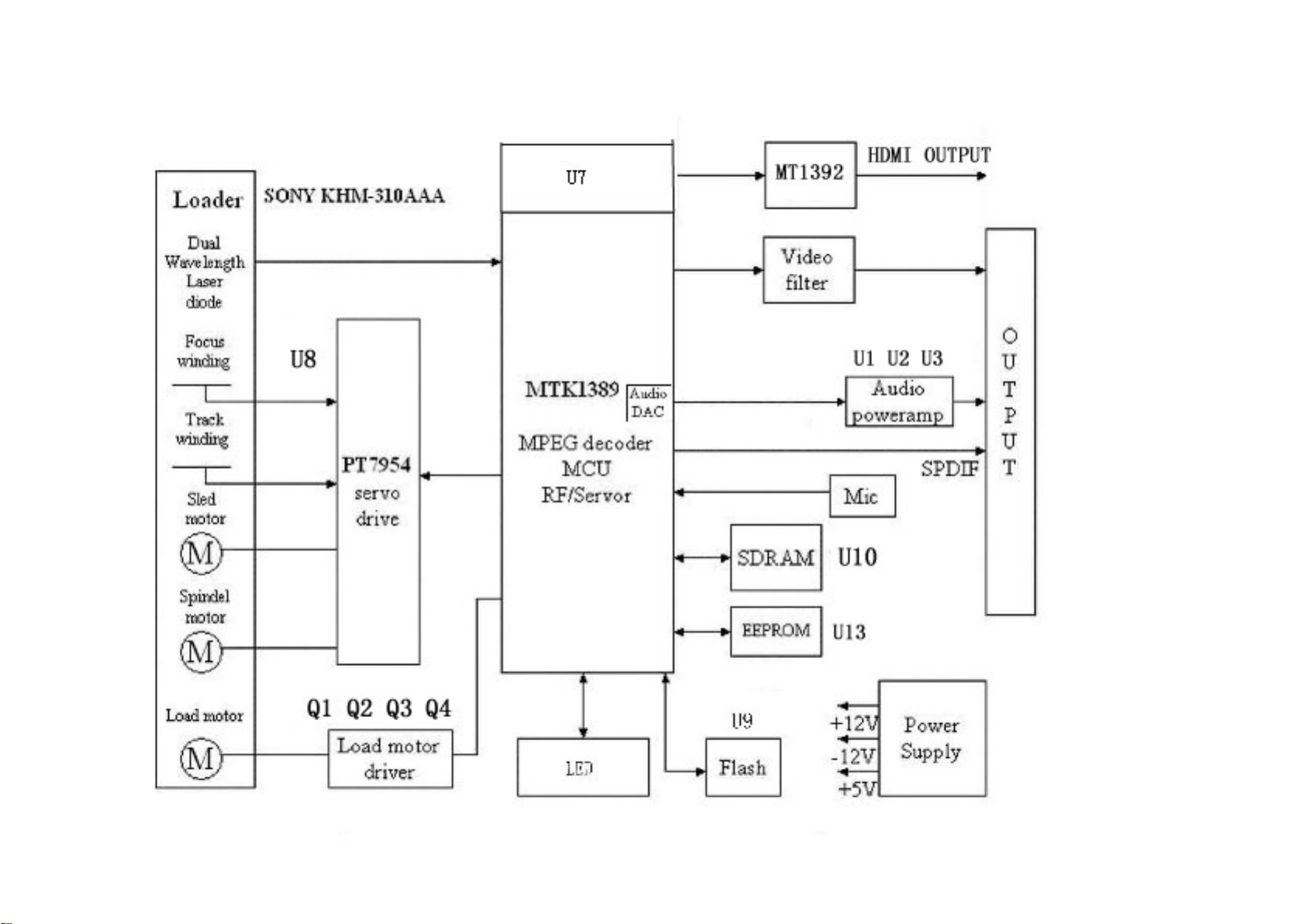
PART 2 KEY Ics And Assemblies
On Main Board On power board
Serial
No
Position Type
Serial
no
position
type
1 U
5 U14
AMS1117 1
2A0565/FSDH321
2 U
6 U15
CX1117—3.3 2 PC817/EL817
3
3 KA431
4 U
7
MT
1389DE/H
5 U
8
PT7954
6
On Panel board
7
8 U10 HY57V641620HGT
Serial
no
position
position
9 U
9 KH29LV160BT
1 U1 PT1628
10 U1
3
24C04
11
12 U1
U2 U3
NJM4558
ICS ON MAIN BOARD
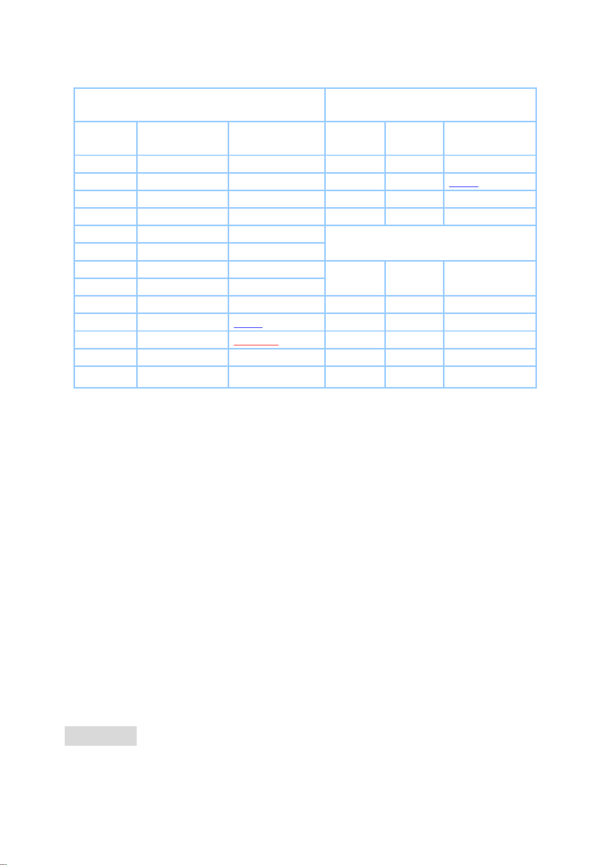
REG1117:800mA and 1A Low Dropout Positive Regulator1.8V, 2.5V, 2.85V,
3.3V, 5V, and Adjustable


Version 1.6 MT1389HD
Specifications are subject to change without notice Control I/O Pin Assignment
2005/11/15
Item
Name
Pin
#
Power-on & IO Status
Original Purpose
GPIO Purpose
Note
1 UP1_2 97 Inout, 4MA, SR, PU, SMT Micro Controller Port 1-2 (>4 Bank)
2 UP1_3 98 Inout, 4MA, SR, PU, SMT Micro Controller Port 1-3 VSCK
3 UP1_4 99 Inout, 4MA, SR, PU, SMT Micro Controller Port 1-4 VSTB
4 UP1_5 100 Inout, 4MA, SR, PU, SMT Micro Controller Port 1-5 VSDA
5 UP1_6 101 Inout, 4MA, SR, PU, SMT Micro Controller Port 1-6 I2C SCK
6 UP1_7 102 Inout, 4MA, SR, PU, SMT Micro Controller Port 1-7 I2C SDA
7 UP3_0 103 Inout, 4MA, SR, PU, SMT Micro Controller Po rt 3-0 ASTB
8 UP3_1 104 Inout, 4MA, SR, PU, SMT Micro Controller Port 3-1 Microphone Detection
9 IOA20 75 Inout, 2~16MA, SR, SMT Flash Address 20 / IO (> 1M)
10 IOA21 87 Input, Pull-Down Flash Address 21 / IO (> 2M) Peripheral Reset
11 SPMCLK 204 Input, Non-pull Master Clock of SPDIF Input 1. MS card detect
12
SPDATA 205 Input, Non-pull
Audio Data of SPDIF Input 1. SD card detect
2. SCART TV Selection
13
SPLRCK 206 Input, Non-pull
Left/Right Channel Clock of SPDIF In 1. SM card detect
2. SCART RGB Selection
14
SPBCK 207 Input, Non-pull
Bit Clock of SPDIF Input 1. CF card detect
2. SCART Aspect Ratio Selection
15
ASDATA3 212 Output, Pull-Down
Audio Serial Data 3 (Cb or Rb/Lb)
1. CF D10(IO)/SD CMD (IO)
2. Audio Mute
Note #4
Note #6
Note #7
16 ASDATA4 214 Output, Pull-Down Audio Serial Data 4 (Downmix L/R)
17 MC_DATA 215 Input, Pull-Down Microphone Serial Input
18
VSYN 181 Input, Non-pull
Vertical Sync. Input/Output
1. CF D01 (IO)/SD DATA0(IO)
Note #1
Note #4
Note #6
Note #7
19
YUV7 180 Input, Non-pull
Video Data Output Bit 7
1. CF D09 (IO)/SD DATA1(IO)
2. Audio Line In
Note #4
Note #6
Note #7
20
HSYN 179 Input, Non-pull
Horizontal Sync. Input/Output
1. CF D02 (IO)/SD DATA2(IO)
Note #1
Note #4
Note #6
Note #7
21
IO_17
(DQM2)
177 Input, Pull-Up
1.CF IORDY (I)/SD DATA3(IO)
Note #2
Note #4
Note #6
Note #7
22
C_0/IO_0
(RD16)
176 Input, Non-pull
1.SM CE- (O)
2. Digital Video output C bit 0
Note #7
23
C_1/IO_1
(RD17)
175 Input, Non-pull
1.CF –RESET (O)
2. Digital Video output C bit 1
Note #7
24
C_2/IO_2
(RD18)
173 Input, Non-pull
1.CF INTRQ (I)/SM CLE (O)
2. Digital Video output C bit 2
Note #3
Note #7
25
C_3/IO_3
(RD19)
172 Input, Non-pull
1.CF –IOWR (O)/SM –WE (O)
2. Digital Video output C bit 3
Note #7

MT1389HD
PRELIMINARY, SUBJECT TO CHANGE WITHOUT NOTICE MTK CONFIDENTIAL, NO DISCLOSURE
Item
Name
Pin
#
Power-on & IO Status
Original Purpose
GPIO Purpose
Note
26
C_4/IO_4
(RD20)
171 Input, Non-pull
1.CF –IORD (O)/SM –RE (O)
2. Digital Video output C bit 4
Note #7
27
C_5/IO_5
(RD21)
169 Input, Non-pull
1.CF –CS1 (O)
2. Digital Video output C bit 5
Note #7
28
C_6/IO_6
(RD22)
168 Input, Non-pull
1.CF –CS0 (O)
2. Digital Video output C bit 6
Note #7
29
C_7/IO_7
(RD23)
167 Input, Non-pull
1.CF D15 (IO)/SM –R_B(IO)
2. Digital Video output C bit 7
Note #5
Note #7
30 YUVCLK
/IO_8
(DQM3)
166 Input, Pull-Up
1.CF D07 (IO)
2.Digital Video Clock output
Note #7
31
Y_0/IO_9
(RD24)
165 Input, Non-pull
1.CF D14 (IO)/SM D4 (IO)
2. Digital Video output Y bit 0
Note #7
32
Y_1/IO_10
(RD25)
164 Input, Non-pull
1.CF D06 (IO)/SM D3 (IO)
2. Digital Video output Y bit 1
Note #7
33
Y_2/IO_11
(RD26)
163 Input, Non-pull
1.CF D13 (IO)/SM D5 (IO)
2. Digital Video output Y bit 2
Note #7
34
Y_3/IO_12
(RD27)
162 Input, Non-pull
1.CF D05 (IO)/SM D2 (IO)
2. Digital Video output Y bit 3
Note #7
35
Y_4/IO_13
(RD28)
161 Input, Non-pull
1.CF D12 (IO)/SM D6 (IO)
2. Digital Video output Y bit 4
Note #7
36
Y_5/IO_14
(RD29)
159 Input, Non-pull
1.CF D04 (IO)/SM D1 (IO)
2. Digital Video output Y bit 5
Note #7
37
Y_6/IO_15
(RD30)
158 Input, Non-pull
1.CF D11 (IO)/SM D7 (IO)
2. Digital Video output Y bit 6
Note #7
38
Y_7/IO_16
(RD31)
157 Input, Non-pull
1.CF D03 (IO)/SM D0 (IO)
2. Digital Video output Y bit 7
Note #7
39 IO_18
(DQS1)
130 Input, Non-pull
Sled fglimit
40 IO_19
(DQS0)
112 Input, Non-pull
SERVO IOA Laser Switch
41 TDI 51 Input, Non-pull JTAG Data In SERVO TROUT Note #1
42 TMS 52 Input, Non-pull Test Mode Select SERVO TRIN Note #1
43 TCK 53 Input, Non-pull JTAG Clock SERVO STBY Note #1
44 TDO 54 Input, Non-pull JTAG Data Out SERVO TRCLOSE (Only GPO) Note #1
45
ASDATA2/
GPO_0
203 Input, Pull-Down Audio Serial Data 2 (C/Sub) 1.MS CLK (O)
GPO only
Note #6
Note #7
46
ASDATA1
/ GPO_1
202 Input, Pull-Down Audio Serial Data 1 (Ls/Rs)
1.CF A00 (O)/MS BS(O)/SM –WP
(O)
GPO only
Note #6
Note #7
47
ASDATA0
/ GPO_2
197 Input, Pull-Down Audio Serial Data 0 (L/R) 1. SD CLK(O)
GPO only
Note #6
Note #7
48
GPIO_3 201 Input, Pull-Down
1. CF D08 (IO)/MS DATA0 (IO)
Note #6
Note #7
49 GPIO_4 200 Input, Pull-Down
1. CF D00 (IO)/MS DATA1 (IO)
Note #6
Note #7

MT1389HD
PRELIMINARY, SUBJECT TO CHANGE WITHOUT NOTICE MTK CONFIDENTIAL, NO DISCLOSURE
Item
Name
Pin
#
Power-on & IO Status
Original Purpose
GPIO Purpose
Note
50 RCLKB
(GPIO_5)
199 Input, Pull-Up
1. CF A01 (O)/MS DATA2 (IO)
Note #6
Note #7
51 RVREF
(GPIO_6)
198 Input, Pull-Up
1. CF A02 (O)/MS DATA3 (IO)/SM
ALE (O)
Note #6
Note #7
52 ARF/
AGPIO_0
222 Input, Non-pull
AUDIO DAC Subwoofer channel
output
GPIO
53 ARS/
ASDATA3
223 Input, Non-pull
AUDIO DAC right s urround channel
output
GPIO
54 AR/
ASDATA1
224 Input, Non-pull
AUDIO DAC right channel output
GPIO
55 AL/
ASDATA2
226 Input, Non-pull
AUDIO DAC left channel output
GPIO
56 ALS/
ASDATA0
227 Input, Non-pull
AUDIO DAC left surround channel
output
GPIO
57 ALF/
AGPIO_1
228 Input, Non-pull
AUDIO DAC Center chann e l ou tput
GPIO
History: 1.3 Finalized the 6-in-1 pins assignment
1.4 The same with 1.3.
1.5 Renaming the RD16~RD31 and define the HDMI and card reader pins.
Notice :
Note #1 :
These pins should not Pull-high to 5V.
3.3V is ok for that.
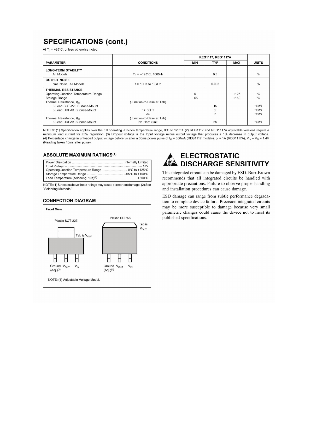
Item Name Pin# Max. Input voltage
1
FG
50 3.3
2
TDI
51 3.3
3
TMS
52 3.3
4
TCK
53 3.3
5
TDO
54 3.3
6
VSYN
181 3.3
7
HSYN
179 3.3
Note #2:
Pull-high to 3.3V by > 10K Ohms on the board when CF is applied.
Note #3:
Pull-low to ground by > 10K Ohms on the board when CF is applied.
Note #4:
Pull-high to 3.3V by 10K Ohms on the board when SD is applied.
Note #5:
Pull-high to 3.3V by 10K?? Ohms on the board when SMC is applied.
Note #6:
4-in-1 related pins.(MS/MS Pro/SD/MMC)
Note #7:
6-in-1 related pins.(MS/MS Pro/SD/MMC/CF/SM)

Abbr. :
SR : Slew Rate
PU : Pull Up
PD : Pull Down
SMT : Schmitt Trigger
2MA~16MA : Output buffer driving strength.
Pin Main Alt. Type Description
RF Interface ( 26 )
231 RFGND18 Ground Analog ground
232 RFVDD18 Power Analog power 1.8V
252 OSP Analog output RF Offset cancellation capacitor connecting
253 OSN Analog output RF Offset cancellation capacitor connecting
254 RFGC Analog output RF AGC loop capacitor connecting for DVD-ROM
255 IREF Analog Input
Current reference input. It generates reference current for
RF path. Connect an external 15K resistor to this pin and
AVSS.
256 AVDD3 Power Analog power 3.3V
1 AGND Ground Analog ground
2 DVDA Analog Input AC coupled input path A
3 DVDB Analog Input AC coupled input path B
4 DVDC A nalog I nput AC coupled input path C
5 DVDD Analog Input AC coupled input path D
6 DVDRFIP Analog Input AC coupled DVD RF signal input RFIP
7 DVDRFIN Analog I nput AC coupled DVD RF signal input RFIN
8 MA Analog Input DC coupled main-beam RF signal input A
9 MB Analog Input DC coupled main-beam RF signal input B
10 MC Analog Input DC coupled main-beam RF signal input C
11 MD Analog Input DC coupled main-beam RF signal input D
12 SA Analog Input DC coupled sub-beam RF signal input A
13 SB Analog Input DC coupled sub-beam RF signal input B
14 SC Analog Input DC coupled sub-beam RF signal input C
15 SD Analog Input DC coupled sub-beam RF signal input D
16 CDFON Analog Input CD focusing error negative input
17 CDFOP Analog Input CD focusing error positive input
18 TNI Analog Input 3 beam satellite PD signal nega tive input
19 TPI Analog Input 3 beam satellite PD signal positive input
ALPC ( 4 )

MTK Confidential A
Pin Main Alt. Type Description
20 MDI1 Analog Input Laser power monitor input
21 MDI2 Analog Input Laser power monitor input
22 LDO2 Analog Output Laser driver output
23 LDO1 Analog Output Laser driver output
ADC Power ( 2 )
244 ADCVDD3 Power Analog 3.3V Power for ADC
245 ADCVSS Ground Analog ground for ADC
VPLL (3)
43 VPLLVSS Ground Analog ground for VPLL
44 CAPPAD Analog Inout VPLL External Capacitance connection
45 VPLLVDD3 Power Analog 3.3V Power for VPLL
Reference Voltage ( 3 )
28 V2REFO Analog output Reference voltage 2.8V
29 V20 Analog output Reference voltage 2.0V
30 VREFO Analog output Reference voltage 1.4V
Analog Monitor Output ( 7 )
24 SVDD3 Power Analog power 3.3V
25 CSO RFOP Analog output
1) Central servo
2) Positive main beam summing output
26 RFLVL RFON Analog output
1) RFRP low pass, or
2) Negative main beam summing output
27 SGND Ground Analog ground
31 FEO Analog output Focus error monitor output
32 TEO Analog output Tracking error monitor output
33 TEZISLV Analog output TE Slicing Level
Analog Servo Interface ( 6 )
246 RFVDD3 Power Analog Power
247 RFRPDC Analog output RF ripple detect output
248 RFRPAC Analog Input RF ripple detect input(through AC-coupling)
249 HRFZC Analog Input High frequency RF ripple zero crossing
250 CRTPLP Analog output Defect level filter capacitor connecting
251 RFGND Ground Analog Power
RF Data PLL Interface ( 9 )
235 JITFO Analog output The output terminal of RF jitter meter.
236 JITFN Analog Input The input terminal of RF jitter meter.
237 PLLVSS Ground Ground pin for data PLL and related analog circuitry.

MTK Confidential A
Pin Main Alt. Type Description
238 IDACEXLP Analog output Data PLL DAC Low-pass filter
239 PLLVDD3 Power Power pin for data PLL and related analog circuitry.
240 LPFON Analog Output The negative output of loop filter amplifier
241 LPFIP Analog Input The positive input terminal of loop filter amplifier.
242 LPFIN Analog Input The negative input terminal of loop filter amplifier.
243 LPFOP Analog Output The positive output of loop filter amplifier
Motor and Actuator Driver Interface ( 10 )
34 OP_OUT Analog output Op amp output.
35 OP_INN Analog input Op amp negative input
36 OP_INP Analog input Op amp positive input
37 DMO Analog Output Disk motor control output. PWM output.
38 FMO Analog Output Feed motor control. PWM output.
39
TROPENPW
M
Analog Output Tray PWM output / Tray open output.
40 PWMOUT1 V_ADIN9 Analog Output
1) 1
st
General PWM output, or
2) Version AD input 9
41 TRO Analog Output
Tracking servo output. PDM output of tracking servo
compensator.
42 FOO Analog Output Focus servo output. PDM output of focus servo compensator
50
FG
(Diogital pin)
V_ADIN8
LVTTL 3.3V Input,
Schmitt Input, pull
up , with analog
input path for
V_ADIN8
1) Motor Hall sensor input, or
2) Version AD input 8
General Power/Ground ( 18 )
55,93,
142,160,
174, 213
DVDD18 Power 1.8V power pin for internal digital circuitry
81,178 DVSS Ground 1.8V Ground pin for internal digital circuitry
65,96,118,
131,145,156,
170, 208
DVDD3 Power 3.3V power pin for internal digital circuitry
90, 148 DVSS Ground 3.3V Ground pin for internal digital circuitry
Micro Controller and Flash Interface ( 48 )
62 HIGHA0
Inout
2~16MA, SR
PU
Microcontroller address 8
74 HIGHA1
Inout
2~16MA, SR
PU
Microcontroller address 9
MT1389HD
PRELIMINARY, SUBJECT TO CHANGE WITHOUT NOTICE MTK CONFIDENTIAL, NO DISCLOSURE
4
MTK Confidential A
Pin Main Alt. Type Description
73 HIGHA2
Inout
2~16MA, SR
PU
Microcontroller address 10
72 HIGHA3
Inout
2~16MA, SR
PU
Microcontroller address 11
71 HIGHA4
Inout
2~16MA, SR
PU
Microcontroller address 12
70 HIGHA5
Inout
2~16MA, SR
PU
Microcontroller address 13
69 HIGHA6
Inout
2~16MA, SR
PU
Microcontroller address 14
68 HIGHA7
Inout
2~16MA, SR
PU
Microcontroller address 15
89 AD7
Inout
2~16MA, SR
Microcontroller address/data 7
86 AD6
Inout
2~16MA, SR
Microcontroller address/data 6
85 AD5
Inout
2~16MA, SR
Microcontroller address/data 5
84 AD4
Inout
2~16MA, SR
Microcontroller address/data 4
83 AD3
Inout
2~16MA, SR
Microcontroller address/data 3
82 AD2
Inout
2~16MA, SR
Microcontroller address/data 2
80 AD1
Inout
2~16MA, SR
Microcontroller address/data 1
79 AD0
Inout
2~16MA, SR
Microcontroller address/data 0
92 IOA0
Inout
2~16MA, SR
PU
Microcontroller address 0 / IO
77 IOA1
Inout
2~16MA, SR
PU
Microcontroller address 1 / IO
56
IOA2
Inout
2~16MA, SR
PU
Microcontroller address 2 / IO
57 IOA3
Inout
2~16MA, SR
PU
Microcontroller address 3 / IO

MT1389HD
PRELIMINARY, SUBJECT TO CHANGE WITHOUT NOTICE MTK CONFIDENTIAL, NO DISCLOSURE
5
MTK Confidential A
Pin Main Alt. Type Description
58 IOA4
Inout
2~16MA, SR
PU
Microcontroller address 4 / IO
59 IOA5
Inout
2~16MA, SR
PU
Microcontroller address 5 / IO
60 IOA6
Inout
2~16MA, SR
PU
Microcontroller address 6 / IO
61 IOA7
Inout
2~16MA, SR
PU
Microcontroller address 7 / IO
67 A16
Output
2~16MA, SR
Flash address 16
91 A17
Output
2~16MA, SR
Flash address 17
63 IOA18
Inout
2~16MA, SR
SMT
Flash address 18 / IO
64 IOA19
Inout
2~16MA, SR
SMT
Flash address 19 / IO
75 IOA20
Inout
2~16MA, SR
SMT
Flash address 20 / IO
87 IOA21
Inout
2~16MA, SR
SMT
1) Flash address 21 / IO
2) While External FLASH size <= 2MB:
I) GPIO
88 ALE
Inout
2~16MA, SR
PU, SMT
Microcontroller address latch enable
78 IOOE#
Inout
2~16MA, SR
SMT
Flash output enable, active low / IO
66 IOWR#
Inout
2~16MA, SR
SMT
Flash write enable, active low / IO
76 IOCS#
Inout
2~16MA, SR
PU, SMT
Flash chip select, active low / IO
94 UWR#
Inout
2~16MA, SR
PU, SMT
Microcontroller write strobe, active low
95 URD#
Inout
2~16MA, SR
PU, SMT
Microcontroller read strobe, active low

MT1389HD
PRELIMINARY, SUBJECT TO CHANGE WITHOUT NOTICE MTK CONFIDENTIAL, NO DISCLOSURE
6
MTK Confidential A
Pin Main Alt. Type Description
97 UP1_2
Inout
4MA, SR
PU, SMT
Microcontroller port 1-2
98 UP1_3
Inout
4MA, SR
PU, SMT
Microcontroller port 1-3
99 UP1_4
Inout
4MA, SR
PU, SMT
Microcontroller port 1-4
100 UP1_5
Inout
4MA, SR
PU, SMT
Microcontroller port 1-5
101 UP1_6 SCL
Inout
4MA, SR
PU, SMT
1) Microcontroller port 1-6
2) I
2
C clock pin
102 UP1_7 SDA
Inout
4MA, SR
PU, SMT
1) Microcontroller port 1-7
2) I
2
C data pin
103 UP3_0 RXD
Inout
4MA, SR
PU, SMT
1) Microcontroller port 3-0
2) 8032 RS232 RXD
104 UP3_1 TXD
Inout
4MA, SR
PU, SMT
1) Microcontroller port 3-1
2) 8032 RS232 TXD
105 UP3_4
RXD
SCL
Inout
4MA, SR
PU, SMT
1) Microcontroller port 3-4
2) Hardwired RD232 RXD
3) I
2
C clock pin
106 UP3_5
TXD
SDA
Inout
4MA, SR
PU, SMT
1) Microcontroller port 3-5
2) Hardwired RD232 TXD
3) I
2
C data pin
109 IR
Input
SMT
IR control signal input
110 INT0#
Inout
2~16MA, SR
PU, SMT
Microcontroller external interrupt 0, active low
Audio interface ( 28 )
204 SPMCLK SCLK0
Inout
Non-pull
1) Audio DAC master clock of SPDIF input
2) While SPDIF input is not used:
I) Serial interface port 0 clock pin
II) GPIO
205 SPDATA SDIN0
Inout
Non-pull
1) Audio data of SPDIF input
2) While SPDIF input is not used:
I) Serial interface port 0 data-in
II) GPIO
MT1389HD
PRELIMINARY, SUBJECT TO CHANGE WITHOUT NOTICE MTK CONFIDENTIAL, NO DISCLOSURE
7
MTK Confidential A
Pin Main Alt. Type Description
206 SPLRCK SDO0
Inout
Non-pull
1) Audio left/right channel clock of SPDIF input
2) While SPDIF input is not used:
I) Serial interface port 0 data-out
II) GPIO
207 SPBCK
SDCS0
ASDATA5
Inout
Non-pull
1) Audio bit clock of SPDIF input
2) While SPDIF input is not used:
I) Serial interface port 0 chip select
II) Audio serial data 5 part I : DSD data sub-woofer
channel or Microphone output
III) GPIO
209 ALRCK
Inout
4MA,
PD, SMT
1) Audio left/right channel clock
2) Trap value in power-on reset:
I) 1 : use external 373
II) 0: use internal 373
210 ABCK Fs64
Output
4MA
Non-pull
1) Audio bit clock
2) Phase de-modulation
211 ACLK
Inout
4MA
Non-pull
Audio DAC master clock
197 ASDATA0
Inout
4MA
PD SMT
1) Audio serial data 0 (Front-Left/Front-Right)
2) DSD data left channel
3) Trap value in power-on reset :
I) 1 : manufactory test mode
II) 0 : normal operation
4) While using external channels:
I) GPO_2
202 ASDATA1
Inout
4MA
PD SMT
1) Audio serial data 1 (Left-Surround/Right-Surround)
2) DSD data right channel
3) Trap value in power-on reset :
I) 1 : manufactory test mode
II) 0 : normal operation
4) While using external channels:
I) GPO_1
203 ASDATA2
Inout
4MA
PD SMT
1) Audio serial data 2 (Center/LFE)
2) DSD data left surround channel
3) Trap value in power-on reset :
I) 1 : manufactory test mode
II) 0 : normal operation
4) While using external channels:
I) GPO_0

MT1389HD
PRELIMINARY, SUBJECT TO CHANGE WITHOUT NOTICE MTK CONFIDENTIAL, NO DISCLOSURE
8
MTK Confidential A
Pin Main Alt. Type Description
212 ASDATA3
Inout
4MA
PD SMT
1) Audio serial data 3 (Center-back/
Center-left-back/Center-right-back, in 6.1 or 7.1 mode)
2) DSD data right surround channel
3) Trap value in power-on reset :
I) 1 : manufactory test mode
II) 0 : normal operation
4) While only 2 channels output:
I) GPIO
214 ASDATA4 INT1#
Inout
4MA
PD SMT
1) Audio serial data 4 (Down-mixed Left/Right)
2) DSD data center channel
3) Trap value in power-on reset :
I) 1 : manufactory test mode
II) 0 : normal operation
4) While only 2 channels output:
I) Microcontroller exte rnal interrupt 1
II) GPIO
215 MC_DATA INT2#
Inout
PD SMT
1) Microphone serial input
2) While not support Microphone:
I) Microcontroller exte rnal interrupt 2
II) GPIO
216 SPDIF
Output
2~16MA,
SR : ON/OFF
Non-pull
SPDIF output
217 APLLVDD3 Power 3.3V Power pin for audio clock circuitry
218 APLLCAP Analog Inout APLL External Capacitance connection
219 APLLVSS Ground Ground pin for audio clock circuitry
220 ADACVSS2 Ground Ground pin for AUDIO DAC circuitry
221 ADACVSS1 Ground Ground pin for AUDIO DAC circuitry
222 ARF GPIO Output
1) AUDIO DAC Sub-woofer channel output
2) While internal AUDIO DAC not used: GPIO
223 ARS GPIO Output
1) AUDIO DAC Right Surround channel output
2) While internal AUDIO DAC not used:
a. SDATA3
b. GPIO
224 AR GPIO Output
1) AUDIO DAC Right channel output
2) While internal AUDIO DAC not used:
a. SDATA1
b. GPIO
225 AVCM Analog AUDIO DAC reference voltage
226 AL GPIO Output
1) AUDIO DAC Left Surround channel output
2) While internal AUDIO DAC not used:
a. SDATA2
b. GPIO
MT1389HD
PRELIMINARY, SUBJECT TO CHANGE WITHOUT NOTICE MTK CONFIDENTIAL, NO DISCLOSURE
9
MTK Confidential A
Pin Main Alt. Type Description
227 ALS GPIO Output
1) AUDIO DAC Left Surround channel output
2) While internal AUDIO DAC not used:
a. SDATA0
b. GPIO
228 ALF GPIO Output
1) AUDIO DAC Center channel output
2) While internal AUDIO DAC not used: GPIO
229 ADACVDD1 Power 3.3V power pin for AUDIO DAC circuitry
230 ADACVDD2 Power 3.3V power pin for AUDIO DAC circuitry
Video Interface ( 18 )
196 DACVDDC Power 3.3V power pin for VIDEO DAC circuitry
195 VREF Analog Bandgap reference voltage
194 FS Analog Full scale adjustment
193 YUV0 CIN
Output
4MA, SR
1) Video data output bit 0
2) Compensation capacitor
192 DACVSSC Ground Ground pin for VIDEO DAC circuitry
191 YUV1 Y
Output
4MA, SR
1) Video data output bit 1
2) Analog Y output
190 DACVDDB Power 3.3V power pin for VIDEO DAC circuitry
189 YUV2 C
Output
4MA, SR
1) Video data output bit 2
2) Analog chroma output
188 DACVSSB Ground Ground pin for VIDEO DAC circuitry
187 YUV3 CVBS
Output
4MA, SR
1) Video data output bit 3
2) Analog composite output
186 DACVDDA Power 3.3V power pin for VIDEO DAC circuitry
185 YUV4 Y/G
Output
4MA, SR
1) Video data output bit 4
2) Green or Y
184 DACVSSA Ground Ground pin for VIDEO DAC circuitry
183 YUV5 B/Cb/Pb
Output
4MA, SR
1) Video data output bit 5
2) Blue or CB
182 YUV6 R/Cr/Pr
Output
4MA, SR
1) Video data output bit 6
2) Red or CR
181 VSYN V_ADIN1
Inout
4MA, SR
SMT
Non-pull
1) Vertical sync input/output
2) While no External TV-encoder:
I) Vertical sync for video-input
II) Version AD input port 1
III) GPIO
180 YUV7
INT3#
ASDATA5
Inout
4MA, SR
SMT
Non-pull
1) Video data output bit 7
2) While no External TV-encoder:
I) Microcontroller exte rnal interrupt 3
II) Audio serial data 5 part II : DSD data sub-woofer
channel or Microphone output
III) GPIO

MT1389HD
PRELIMINARY, SUBJECT TO CHANGE WITHOUT NOTICE MTK CONFIDENTIAL, NO DISCLOSURE
10
MTK Confidential A
Pin Main Alt. Type Description
179 HSYN
INT4#
V_ADIN2
Inout
4MA, SR
SMT
Non-pull
1) Horizontal sync input/output
2) While no External TV-encoder:
I) Horizontal sync for video-input
II) Microcontroller external interrupt 4
III) Version AD input port 2
IV) GPIO
MISC ( 12 )
46 USB_VSS USB Ground USB ground pin
47 USBP Analog Inout USB port DPLUS analog pin
48 USBM Analog Inout USB port DMINUS analog pin
49 USB_VDD3 USB Power USB Power pin 3.3V
108 PRST#
Input
PU, SMT
Power on reset input, active low
107 ICE
Input
PD, SMT
Microcontroller ICE mode enable
233 XTALO Output 27M crystal out
234 XTALI Input
27M crystal in
201 GPIO_3
Inout
Pull-Down
GPIO
200 GPIO_4
Inout
Pull-Down
GPIO
199 RCLKB GPIO_5
Inout
Pull-Up
GPIO
198
RVREF GPIO_6
Inout
Pull-Up
GPIO
Dram Interface ( 58 ) ( Sorted by position )
176 C_0
IO_0
(RD16)
Inout
Non-pull
1) Digital Video output C bit 0
2) GPIO
175 C_1
IO_1
(RD17)
Inout
Non-pull
1) Digital Video output C bit 1
2) GPIO
173 C_2
IO_2
(RD18)
Inout
Non-pull
1) Digital Video output C bit 2
2) GPIO
172 C_3
IO_3
(RD19)
Inout
Non-pull
1) Digital Video output C bit 3
2) GPIO
171 C_4
IO_4
(RD20)
Inout
Non-pull
1) Digital Video output C bit 4
2) GPIO
169 C_5
IO_5
(RD21)
Inout
Non-pull
1) Digital Video output C bit 5
2) GPIO
168 C_6
IO_6
(RD22)
Inout
Non-pull
1) Digital Video output C bit 6
2) GPIO
167 C_7
IO_7
(RD23)
Inout
Non-pull
1) Digital Video output C bit 7
2) GPIO

MT1389HD
PRELIMINARY, SUBJECT TO CHANGE WITHOUT NOTICE MTK CONFIDENTIAL, NO DISCLOSURE
11
MTK Confidential A
Pin Main Alt. Type Description
177 IO_17 (DQM2)
Inout
Pull-Up
GPIO
166 YUVCLK
IO_8
(DQM3)
Inout
Pull-Up
1) Digital Video output Clock
2) GPIO
165
Y_0
IO_9
(RD24)
Inout
Non-pull
1) Digital Video output Y bit 0
2) GPIO
164
Y_1
IO_10
(RD25)
Inout
Non-pull
1) Digital Video output Y bit 1
2) GPIO
163
Y_2
IO_11
(RD26)
Inout
Non-pull
1) Digital Video output Y bit 2
2) GPIO
162
Y_3
IO_12
(RD27)
Inout
Non-pull
1) Digital Video output Y bit 3
2) GPIO
161
Y_4
IO_13
(RD28)
Inout
Non-pull
1) Digital Video output Y bit 4
2) GPIO
159
Y_5
IO_14
(RD29)
Inout
Non-pull
1) Digital Video output Y bit 5
2) GPIO
158
Y_6
IO_15
(RD30)
Inout
Non-pull
1) Digital Video output Y bit 6
2) GPIO
157
Y_7
IO_16
(RD31)
Inout
Non-pull
1) Digital Video output Y bit 7
2) GPIO
155 RA4
Inout
DRAM address 4
154 RA5
Inout
DRAM address 5
153 RA6
Inout
DRAM address 6
152 RA7
Inout
DRAM address 7
151 RA8
Inout
DRAM address 8
150 RA9
Inout
DRAM address 9
149 RA11
Inout
Pull-Down
DRAM address bit 11
147 CKE output DRAM clock enable
146 RCLK Inout Dram clock
144 RA3
Inout
DRAM address 3
143 RA2
Inout
DRAM address 2
141 RA1
Inout
DRAM address 1
140 RA0
Inout
DRAM address 0
139 RA10
Inout
DRAM address 10
138 BA1
Inout
DRAM bank address 1
137 BA0
Inout
DRAM bank address 0
136 RCS#
output
DRAM chip select, active low
135 RAS#
output
DRAM row address strobe, active low
134 CAS#
output
DRAM column address strobe, active low
133 RWE#
output
DRAM Write enable, active low
132 DQM1
Inout
Data mask 1
130 IO_18 (DQS1)
Inout
Non-pull
GPIO
129 RD8
Inout
DRAM data 8
128 RD9
Inout
DRAM data 9

MT1389HD
PRELIMINARY, SUBJECT TO CHANGE WITHOUT NOTICE MTK CONFIDENTIAL, NO DISCLOSURE
12
MTK Confidential A
Pin Main Alt. Type Description
127 RD10
Inout
DRAM data 10
126 RD11
Inout
DRAM data 11
125 RD12
Inout
DRAM data 12
124 RD13
Inout
DRAM data 13
123 RD14
Inout
DRAM data 14
122 RD15
Inout
DRAM data 15
121 RD0
Inout
DRAM data 0
120 RD1
Inout
DRAM data 1
119 RD2
Inout
DRAM data 2
117 RD3
Inout
DRAM data 3
116 RD4
Inout
DRAM data 4
115 RD5
Inout
DRAM data 5
114 RD6
Inout
DRAM data 6
113 RD7
Inout
DRAM data 7
112 IO_19 (DQS0)
Inout
Non-pull
GPIO
111 DQM0
Inout
Data mask 0
JTAG Interface( 4 )
51 TDI
V_ADIN4
Inout
Non-pull
1) Serial interface port 3 data-out
2) Version AD input port 4
3) GPIO
52 TMS
V_ADIN5
Inout
Non-pull
1) Serial interface port 3 data-in
2) Version AD input port 5
3) GPIO
53 TCK
V_ADIN6
Inout
Non-pull
1) Serial interface port 3 clock pin
2) Version AD input port 6
3) GPIO
54 TDO
V_ADIN7
Inout
Non-pull
1) Serial interface port 3 chip-select
2) Version AD input port 7
3) GPO
Note:
1. The Main column is the main function, Alt. Means alternative function.
2. The multi-function GPIO pins are set to green characters.
3. The video input por t a nd external TV en c oder mode can not bo th use CCIR-601 mode, at least one of them
should be in C CIR-65 6 mode.
4. Following is a summary of modified pins.
(a) Pin 48, 49, 50, 51 are no longer for JTAG functions.
(b) V_ADIN0 and V_ADIN3 is not available.
Revision History:
Date Version Content
2004-09-14 1.0 z Document Initial
2004-09-17 1.1 z Reorder all pins based on pinV1.1

MTK Confidential A
2004-09-30 1.2 z Reorder all pins ba sed on pinV1.2 for better Placement
2004-10-04 1.3 z Update the pull status of IO
2004-11-08 1.4
z Change the 5.1CH ADAC p ins positions fo r L-group and R-gro up
being together.(pin 223~pi n228)
z pin43, pin45 change order to pin43(VPLLVSS),
pin45(VPLLVDD)
2004-11-15 1.5
z Add ASDAT A3 function on pin223(PAD_ARS)
z Renaming the RD16~RD31, DQM[3:2], DQS[1:0] as IO_[19:0]
z Pin229 was changed as ADACVDD1
z Pin230 was changed as ADACVDD2
z
 Loading…

-
Contents
-
Table of Contents
-
Troubleshooting
-
Bookmarks
Quick Links
GENERAL INFORMATION
00
TABLE OF CONTENTS
DIMENSIONS ………………………………………………….. 3
SPECIFICATIONS ……………………………………………. 4
VEHICLE IDENTIFICATION ……………………………….. 6
MAINTENANCE SCHEDULE …………………………….. 9
RECOMMENDED FLUIDS AND LUBRICANTS …… 11
Chapters
Troubleshooting
Related Manuals for SSANGYONG Kyron
Summary of Contents for SSANGYONG Kyron
Welcome to the Auto Repair Manuals.

- Forum
- Легковые автомобили
- SsangYong
- SsangYong Kyron руководство по ремонту

Thread: SsangYong Kyron руководство по ремонту
5 stars based on
2 reviews
-
SsangYong Kyron — руководство по ремонту автомобиля
SsangYong Kyron — уникальное руководство по ремонту автомобиля.
Книга является руководством по самостоятельному ремонту и техническому обслуживанию автовладельцем автомобилей марки SsangYong Kyron оборудованных дизельными двигателями моделей D20DT И D27DT. Также в этой книге указаны схемы электрического оборудования Kyron и перечислены моменты затяжки важных резьбовых соединений этого автомобиля.Год выпуска: 2005
Язык руководства: Русский
Формат книги: PDF
Размер: 174.21 MbСкачать Руководство по ремонту SsangYong Kyron на AutoRepManS:


Similar Threads
-
Replies: 17
Last Post: 25.02.2020, 05:20
-
Replies: 9
Last Post: 29.03.2016, 21:08
-
Replies: 4
Last Post: 12.02.2016, 23:06
-
Replies: 4
Last Post: 08.01.2016, 00:54
-
Replies: 2
Last Post: 08.08.2010, 20:50
Tags for this Thread
Сборник руководств на английском языке по техническому обслуживанию и ремонту + схемы электрооборудования автомобиля SsangYong Kyron.
- Автор: —
- Издательство: SsangYong
- Год издания: 2005-2011
- Страниц: —
- Формат: PDF
- Размер: 2,0 Gb
Руководство по техническому обслуживанию и ремонту автомобиля SsangYong Kyron.
- Автор: —
- Издательство: SsangYong
- Год издания: 2005
- Страниц: —
- Формат: PDF
- Размер: 172,0 Mb

Руководство по техническому обслуживанию и ремонту + каталог расходных запчастей автомобиля SsangYong Kyron с 2005 года выпуска с бензиновыми и дизельными двигателями.
- Автор: —
- Издательство: Легион-Автодата
- Год издания: 2015
- Страниц: 461
- Формат: —
- Размер: —

Руководство по эксплуатации и ремонту автомобиля SsangYong Kyron с 2005 года выпуска с бензиновыми и дизельными двигателями.
- Автор: —
- Издательство: Монолит
- Год издания: —
- Страниц: 474
- Формат: —
- Размер: —
Сборник руководств по эксплуатации и техническому обслуживанию автомобиля SsangYong Kyron.
- Автор: —
- Издательство: SsangYong
- Год издания: —
- Страниц: —
- Формат: PDF
- Размер: 26,0 Mb

Руководство по эксплуатации, техническому обслуживанию и ремонту автомобиля SsangYong Kyron с 2005 года выпуска с дизельными двигателями объемом 2,0/2,7 л.
- Автор: —
- Издательство: Арго-Авто
- Год издания: —
- Страниц: 616
- Формат: —
- Размер: —

SsangYong Kyron (2005-2015) with gasoline and diesel engines: owner’s, workshop, repair and maintenance manual, fuse schematics and wiring diagrams, operating instructions PDF free download
See also:
| Title | File Size | Download Links |
| SsangYong Kyron 2005 Owner’s Manual [PDF] | 252.2Mb | Download |
| SsangYong Kyron 2006 Owner’s Manual [PDF] | 10.5Mb | Download |
| SsangYong Kyron 2006 Service Repair Manual [PDF] | 54.8Mb | Download |
| SsangYong Kyron 2006 User Manual [PDF] | 11Mb | Download |
| SsangYong Kyron 2007 Owner’s Manual [PDF] | 218.6Mb | Download |
| SsangYong Kyron 2008 Owner’s Manual [PDF] | 358.1Mb | Download |
| SsangYong Kyron 2010 Kyron User Manual [PDF] | 11.9Mb | Download |
| SsangYong Kyron 2010 Owner’s Manual [PDF] | 316.5Mb | Download |
| SsangYong Kyron 2015 Owner’s Manual rus [PDF] | 16.6Mb | Download |
| SsangYong Kyron Fault Codes List [PDF] | 62.2kb | Download |
This famous car is called a Korean European for a reason. It organically combines refined oriental style and European avant-garde, traditional quality and the latest developments in the field of mechanical engineering. A comfortable leather interior and convenient controls complete the portrait of a car. Of course, in order for the car to fully meet the expectations of its owner, it is necessary to adhere to simple operating rules, a schedule of preventive checks and, if necessary, immediately repair your SsangYong Kyron. To find out how to perform all the above tasks quickly and with maximum results, the presented manuals for SsangYong Kyron repair, operation and maintenance of cars of this brand will help the driver.
The service manuals describe models equipped with a 2.3 – M161 / 3.2 – M162 gasoline engine, as well as a 2.0 – D20DT / 2.7 – D27DT diesel engine. These manuals will also be of interest to a car service worker who is interested in increasing the speed and efficiency of his work.
These manuals can boast that it contains the most demanded and accurate information, both theoretical and applied, under one cover. This manual well combines an accessible style of presentation, a logical layout of the material and a scientific approach to the automotive topic. In addition, the repair manual for SsangYong Kyron is supplied with high-quality drawings and photographs, due to which the main text becomes clear and much easier to understand.
Mastering the manual begins with general information about SsangYong Kyron. So, in the manual, the design features of a car, its units, components and systems are comprehensively described. Their location, purpose, components (if any) and management principles are indicated. So now the driver will not lose sight of any button or lever. It is also worth paying attention to the fact that the manual contains a complete instruction manual for the SsangYong Kyron, which should be guided by everyone who got behind the wheel. To keep the machine working properly and even after many years of use it looks and behaves like new, it is necessary to carry out regular maintenance of the vehicle. A separate chapter provides an overview of all the necessary checks, their schedule, the tools and materials required for this. The manual covers in detail all issues related to the electrical equipment of the car, including all the electrical circuits of SsangYong Kyron.
SsangYong Kyron background information
SsangYong Kyron is a compact crossover of the South Korean company SsangYong, produced since 2005.
SsangYong Kyron is built on the same platform as the Actyon, however, differs from the co-platform crossover in appearance and interior design.
In 2007, the car was restyled, affecting the front of the body, including lighting, and interior colors.
SsangYong Kyron is equipped with a 2.3-liter gasoline engine (150 hp) and turbodiesels 2.0-liter (141 hp) and 2.7-liter. In addition to manual transmissions, SUVs were equipped with a 5-speed automatic transmission, now equipped with a 6-speed automatic transmission with the possibility of manual shifting.
In Korea, SsangYong Kyron was discontinued in 2011, and the assembly of cars in Vladivostok continued until 2014 (at the end of the conveyor life, a small batch of single-drive cars entered the Russian market). A licensed copy of the model was produced in China under the name Roewe W5.

SsangYong Kyron
Attention! Clicking on the link “download” you agree, after reading, delete the downloaded file from your computer. All content on the site Carmanualsclub.com is taken from free sources and is also freely distributed. If you are the author of this material, then please contact us in order to provide users with a pleasant and convenient alternative, after reading, buying a quality “original” directly from the publisher. The site administration does not bear any responsibility for illegal actions, and any damage incurred by the copyright holders.